Here at Angaza, we’re used to optimizing our hardware designs to be as small, efficient, and as inexpensive as possible. We are able to add pay-as-you-go (PAYG) state monitoring and communications capability to a manufacturer’s existing printed circuit board (PCB) design for less than a dollar, square inch, and milliwatt of cost.
Of course, these optimized designs represent the end state of a successful integration with our hardware partners. The sweet success of shipping can only come after a rigorous development process. One of the key tools used in this process is the development board (or “dev board”), which enables users to build, test, and verify their designs before starting production manufacturing in earnest.
We’ve used a wide variety of third-party development boards to build our own products, and we’ve also built our own internal development board prototypes for years. Recently, we realized that in order to scale out our ever-growing number of hardware partnerships, we needed to produce our own development boards for new partners as well as for existing partners working on new products.
When we first started, we approached the problem like typical engineers, focused on engineering optimizations, as engineers are wont to do … and we learned that this mindset resulted in a poor user experience. With the hope of helping others avoid our experiences, we’re sharing five key lessons we’ve learned about building usable development boards. The best development boards are like Swiss Army knives: they provide easy access to each feature of the onboard hardware and don’t break in spite of accidental misuse. If you heed these lessons in your dev board designs, then like a Swiss Army knife, “usability” may become part of your brand.
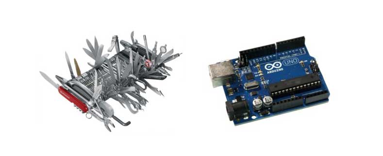
(Left) The Wenger 16999, with 141 functions; (Right) The Arduino Uno development board, with 14 DGPIO.
Image Source: Jim Sheely and Wikimedia.
Building A Usable Development Board
1. Use Standard Connectors For All User Interfaces
If that’s not possible, provide an adapter to your nonstandard connector. Every development board should at the very least include a programming connector, a power connector, and a signal breakout connector.
Never force the user to make a custom connector or perform rework on your development board in order to connect to it.
We made this mistake and it resulted in the loss of our entire inventory of first-revision development boards. We wanted the board to be as small as possible, so we decided to use a half-pitch header for device programming to make everything fit in a fixed 2” x 2” layout area.
The problem was that standard-pitch to half-pitch board-to-board connectors don’t exist. We spelunked Digikey and Mouser; we tried to crimp our own; we strung along a poor sales rep from a connectors company for several months; and finally we broke all of our hacked-together boards from the mechanical stress on the plated through-holes (we had soldered in 22 AWG wires to interface with our programmer pins). Ugh!
In our new design we selected a beautifully ubiquitous standard-pitch header.
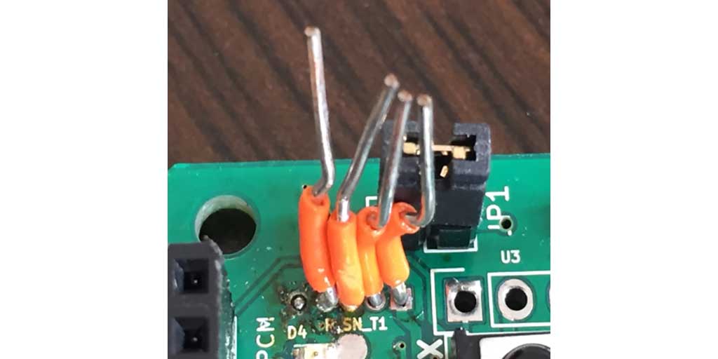 (Above) Jumper wires soldered into the plated through-holes for a hacked-together connector solution.
For each user interface, think critically about how the user is going to connect to it and make sure that it’s easy. If the connector cable is easy to find, consider including it with the development board. It’s likely worth it to your customer to pay a little more to have the required part included than to spend the time and brain space getting it themselves.
2. Account For The Entire Peripheral, Not Just Its Connector
A peripheral is more than its footprint on your PCB. This sounds obvious, but when you’re working on the layout you’re only working with the peripheral board connector, so it’s easy to forget about the orientation and size of what will actually be connecting to that connector.
We decided to include a wired keypad with our dev board to enable manufacturing partners to experiment with our keypad PAYG technology. In our first revision the keypad connector was oriented the wrong way so that the keypad hung over the board. The result was very awkward to use. To help ourselves prevent this mistake moving forward, we made a new footprint in our electronic design automation (EDA) software that included the connector as well as some non-rendering commentary to indicate the direction of the keypad once inserted.
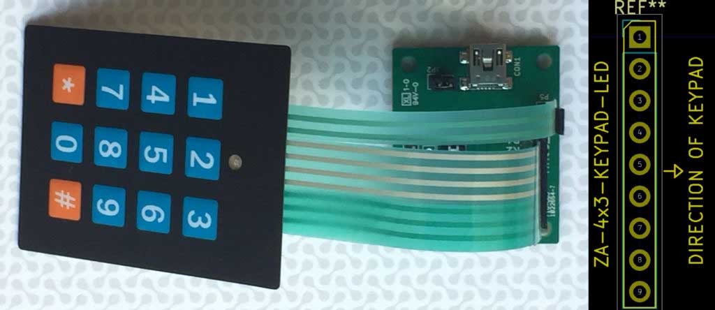 (Left) First version of our board, with a keypad whose ribbon cable had to be twisted or used in the air based on the orientation — awkward; (Right) Follow-on revision of our board, with an annotated electronic design automation (EDA) footprint that reminds the designer of the rest of the peripheral orientation.
The physical size of the peripheral connector is also easy to forget about. Even though two peripheral board connectors can be placed right next to each other on the PCB design, the size of the overmolds of the peripheral connectors may prevent both from being used simultaneously. USB, for example, has been accessorized to the extent that the overmold may come in many different shapes and sizes. Enough clearance should be provided between connectors to allow peripherals with nonstandard overmolds to be used.
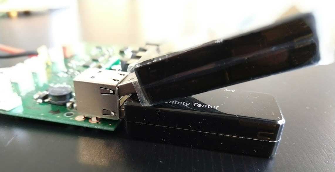 (Above) The USB connectors for this printed circuit board assembly (PCBA) are so close together that it is physically impossible (without breaking something) to insert two of these USB devices simultaneously.
3. Document The Board With Your Silkscreens
Remember, your dev board is not going to be hidden away forever inside an enclosure. And no one likes to read documentation. So, label liberally. An end user should be able to figure out how to connect the power supply and programmer without reading anything but the top of your board.
After frustratingly having to refer to our own documentation too many times to determine our own programmer pinout, we added labels for all switches, power jumpers, and headers. This had the added benefit of discouraging mis-plugs of connectors into places that they shouldn’t be plugged into.
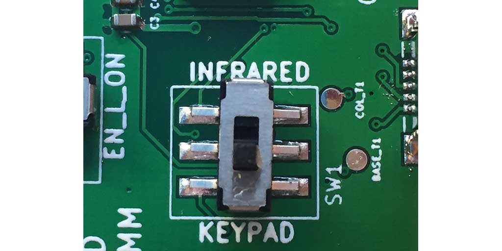
(Above) Clear labeling of the switch functions. Do not make users refer to the manual for the “Operation of SW1.”
4. Invoke Poka-Yoke
Poka-Yoke is an Angaza Word of the Day circa 2014 and refers to design that precludes misuse based on the physical impossibility of that misuse to occur. A great example of common connector misuse is with car battery jumper cables. The proper way to wire cables is to connect the negative terminals together and the positive terminals together. However, due to user confusion in identifying the positive or negative terminals of the batteries, or carelessness in connecting them, the positive terminals could be connected to the negative terminals, resulting in a short-circuit. This could damage the batteries, or worse, the car’s computer system.
Imagine if battery manufacturers put differently-shaped connectors on the terminals. For example, all positive terminals were square-shaped and all negative terminals were circle-shaped. Then you could buy a pair of square- and circle-terminated cables and it would be physically impossible to make a solid connection to the wrong terminals.
USB 1.0/2.0 applies this principle by making its connectors unidirectional. So while it’s sometimes difficult to determine the proper direction, there is only one direction that the connectors can mate and there is no risk for short-circuiting. This saves designers using USB connectors a lot of time and cost because it prevents them from having to handle reverse-voltage protection in their electronics designs. USB-C improves on this by providing a bidirectional connector with a bidirectional (differential, to be precise) electronics protocol as well.
When you’re deciding on mechanical connectors, consider how they could be misused and how the connector design itself can prevent that.
 (Above) USB 1.0/2.0 plugs and sockets are unidirectional connectors that only fit together in one orientation; USB-C plugs and sockets, however, are bidirectional both mechanically and electrically. Image source: Wikimedia.
Poka-yoke isn’t just limited to mechanicals, either. It should also be used with your electrical design. For example, don’t route VDD and GND to adjacent positions in the same header, as this could cause an accidental short-circuit if the user has poor hand-eye coordination when inserting a jumper.
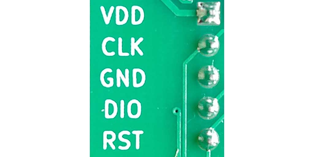
(Above) Close-up of the programming connector on our dev board: even if someone is one off when connecting VDD or GND, a potential short won’t be caused because of the spacing between VDD and GND.
5. Make Rework Easy Where Rework Is Expected
A development board is called a development board for a reason: it should make common modifications easy to save your users from having to make their own hardware in order to test their custom configurations. If a tuning resistor exists in your design, consider changing it to a potentiometer. Provide a large ground pad or multiple ground connections to facilitate debugging. Never use any surface-mount technology (SMT) part smaller than 0603. And don’t forget the test pads.
Before we started going by Angaza, we were known as Angaza Design, a reminder of our roots in user-centric design thinking. Keeping our users in mind is at the core of our work, and it’s part of what’s made us successful thus far. We hope that these tips have helped you keep your own users in mind and thereby improve your dev board design. We’re always happy to take a look at any designs you might have in our spare time; send them our way, and thanks for reading.
Thanks to Alison Polton-Simon.